- 您现在的位置:买卖IC网 > Sheet目录3871 > PIC18F1230T-I/SO (Microchip Technology)IC PIC MCU FLASH 2KX16 18SOIC
PIC18F1230/1330
2009 Microchip Technology Inc.
DS39758D-page 175
16.3
Selecting and Configuring
Acquisition Time
The ADCON2 register allows the user to select an
acquisition time that occurs each time the GO/DONE
bit is set. It also gives users the option to use an
automatically determined acquisition time.
Acquisition time may be set with the ACQT2:ACQT0 bits
(ADCON2<5:3>), which provide a range of 2 to 20 TAD.
When the GO/DONE bit is set, the A/D module
continues to sample the input for the selected acquisition
time, then automatically begins a conversion. Since the
acquisition time is programmed, there may be no need
to wait for an acquisition time between selecting a
channel and setting the GO/DONE bit.
Manual
acquisition
is
selected
when
ACQT2:ACQT0 = 000. When the GO/DONE bit is set,
sampling is stopped and a conversion begins. The user
is responsible for ensuring the required acquisition time
has passed between selecting the desired input
channel and setting the GO/DONE bit. This option is
also the default Reset state of the ACQT2:ACQT0 bits
and is compatible with devices that do not offer
programmable acquisition times.
In either case, when the conversion is completed, the
GO/DONE bit is cleared, the ADIF flag is set and the
A/D begins sampling the currently selected channel
again. If an acquisition time is programmed, there is
nothing to indicate if the acquisition time has ended or
if the conversion has begun.
16.4
Selecting the A/D Conversion
Clock
The A/D conversion time per bit is defined as TAD. The
A/D conversion requires 11 TAD per 10-bit conversion.
The source of the A/D conversion clock is software
selectable. There are seven possible options for TAD:
2 TOSC
4 TOSC
8 TOSC
16 TOSC
32 TOSC
64 TOSC
Internal RC Oscillator
For correct A/D conversions, the A/D conversion clock
(TAD) must be as short as possible, but greater than the
minimum
TAD
(see
parameter
for
more
information).
the device operating frequencies and the A/D clock
source selected.
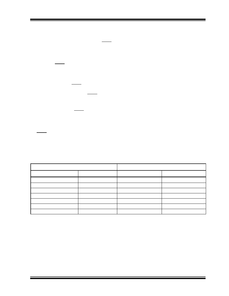
TABLE 16-1:
TAD vs. DEVICE OPERATING FREQUENCIES
AD Clock Source (TAD)
Maximum Device Frequency
Operation
ADCS2:ADCS0
PIC18F1230/1330
PIC18LF1230/1330(4)
2 TOSC
000
2.86 MHz
1.43 MHz
4 TOSC
100
5.71 MHz
2.86 MHz
8 TOSC
001
11.43 MHz
5.72 MHz
16 TOSC
101
22.86 MHz
11.43 MHz
32 TOSC
010
40.0 MHz
22.86 MHz
64 TOSC
110
40.0 MHz
22.86 MHz
RC(3)
x11
1.00 MHz(1)
1.00 MHz(2)
Note 1:
The RC source has a typical TAD time of 1.2 s.
2:
The RC source has a typical TAD time of 2.5 s.
3:
For device frequencies above 1 MHz, the device must be in Sleep for the entire conversion or the A/D
accuracy may be out of specification.
4:
Low-power (PIC18LF1230/1330) devices only.
发布紧急采购,3分钟左右您将得到回复。
相关PDF资料
PIC18F1330T-I/ML
IC PIC MCU FLASH 4KX16 28QFN
PIC18F65J50T-I/PT
IC PIC MCU FLASH 16KX16 64TQFP
PIC18F83J11T-I/PT
IC PIC MCU FLASH 4KX16 80TQFP
PIC16LF627-04/P
IC MCU FLASH 1KX14 COMP 18DIP
PIC18F86J55T-I/PT
IC PIC MCU FLASH 48KX16 80TQFP
PIC18F43K22-I/MV
MCU PIC 8KB FLASH 40QFN
PIC16C55A-04I/P
IC MCU OTP 512X12 28DIP
PIC18LF43K22-I/MV
MCU PIC 8KB FLASH 40UQFN
相关代理商/技术参数
PIC18F1230T-I/SS
功能描述:8位微控制器 -MCU 4KB Flash 256 RAM RoHS:否 制造商:Silicon Labs 核心:8051 处理器系列:C8051F39x 数据总线宽度:8 bit 最大时钟频率:50 MHz 程序存储器大小:16 KB 数据 RAM 大小:1 KB 片上 ADC:Yes 工作电源电压:1.8 V to 3.6 V 工作温度范围:- 40 C to + 105 C 封装 / 箱体:QFN-20 安装风格:SMD/SMT
PIC18F1320-E/ML
功能描述:8位微控制器 -MCU 8KB 256 RAM 16 I/O RoHS:否 制造商:Silicon Labs 核心:8051 处理器系列:C8051F39x 数据总线宽度:8 bit 最大时钟频率:50 MHz 程序存储器大小:16 KB 数据 RAM 大小:1 KB 片上 ADC:Yes 工作电源电压:1.8 V to 3.6 V 工作温度范围:- 40 C to + 105 C 封装 / 箱体:QFN-20 安装风格:SMD/SMT
PIC18F1320-E/P
功能描述:8位微控制器 -MCU 8KB 256 RAM 16 I/O RoHS:否 制造商:Silicon Labs 核心:8051 处理器系列:C8051F39x 数据总线宽度:8 bit 最大时钟频率:50 MHz 程序存储器大小:16 KB 数据 RAM 大小:1 KB 片上 ADC:Yes 工作电源电压:1.8 V to 3.6 V 工作温度范围:- 40 C to + 105 C 封装 / 箱体:QFN-20 安装风格:SMD/SMT
PIC18F1320-E/SO
功能描述:8位微控制器 -MCU 8KB 256 RAM 16 I/O RoHS:否 制造商:Silicon Labs 核心:8051 处理器系列:C8051F39x 数据总线宽度:8 bit 最大时钟频率:50 MHz 程序存储器大小:16 KB 数据 RAM 大小:1 KB 片上 ADC:Yes 工作电源电压:1.8 V to 3.6 V 工作温度范围:- 40 C to + 105 C 封装 / 箱体:QFN-20 安装风格:SMD/SMT
PIC18F1320-E/SS
功能描述:8位微控制器 -MCU 8KB 256 RAM 16 I/O RoHS:否 制造商:Silicon Labs 核心:8051 处理器系列:C8051F39x 数据总线宽度:8 bit 最大时钟频率:50 MHz 程序存储器大小:16 KB 数据 RAM 大小:1 KB 片上 ADC:Yes 工作电源电压:1.8 V to 3.6 V 工作温度范围:- 40 C to + 105 C 封装 / 箱体:QFN-20 安装风格:SMD/SMT
PIC18F1320-H/ML
功能描述:8位微控制器 -MCU 8KB FL 256RAM 16 I/O RoHS:否 制造商:Silicon Labs 核心:8051 处理器系列:C8051F39x 数据总线宽度:8 bit 最大时钟频率:50 MHz 程序存储器大小:16 KB 数据 RAM 大小:1 KB 片上 ADC:Yes 工作电源电压:1.8 V to 3.6 V 工作温度范围:- 40 C to + 105 C 封装 / 箱体:QFN-20 安装风格:SMD/SMT
PIC18F1320-H/P
功能描述:8位微控制器 -MCU 8KB FL 256RAM 16 I/O RoHS:否 制造商:Silicon Labs 核心:8051 处理器系列:C8051F39x 数据总线宽度:8 bit 最大时钟频率:50 MHz 程序存储器大小:16 KB 数据 RAM 大小:1 KB 片上 ADC:Yes 工作电源电压:1.8 V to 3.6 V 工作温度范围:- 40 C to + 105 C 封装 / 箱体:QFN-20 安装风格:SMD/SMT
PIC18F1320-H/SO
功能描述:8位微控制器 -MCU 8KB FL 256RAM 16 I/O RoHS:否 制造商:Silicon Labs 核心:8051 处理器系列:C8051F39x 数据总线宽度:8 bit 最大时钟频率:50 MHz 程序存储器大小:16 KB 数据 RAM 大小:1 KB 片上 ADC:Yes 工作电源电压:1.8 V to 3.6 V 工作温度范围:- 40 C to + 105 C 封装 / 箱体:QFN-20 安装风格:SMD/SMT